
In Augmented Reality and Virtual Reality News
July 11, 2023 – Researchers at Massachusetts Institute of Technology (MIT) have developed a new technique for integrating halide perovskite nanocrystals into nanoscale devices. The technique allows for the precise growth of nanoscale LEDs (nanoLEDs), which could have potential applications in augmented and virtual reality (AR/VR) displays.
Halide perovskites are a group of materials known for their exceptional optoelectronic properties, making them ideal for high-performance solar cells, lasers, and light-emitting diodes (LEDs).
Until now, integrating these materials at the nanoscale has been challenging due to their delicate nature and susceptibility to damage during conventional fabrication processes. To overcome this hurdle, MIT researchers devised a technique that allows for precise on-site growth of individual halide perovskite nanocrystals, with control over their location within 50 nanometers (a sheet of paper is 100,000 nanometers thick).
According to MIT, the innovative new method enables not only precise control over the nanocrystals’ placement but also allows for precise control over their size, which directly affects their characteristics and performance. By growing the material locally with desired features, the need for conventional lithographic patterning steps that could potentially cause damage is eliminated.
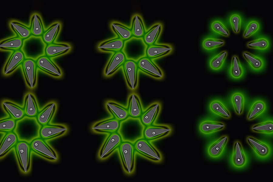
MIT noted that the technique is scalable, versatile, and compatible with conventional fabrication steps, making it suitable for integrating nanocrystals into functional nanoscale devices. Researchers successfully utilized the method to fabricate arrays of nanoscale LEDs (nanoLEDs), which emit light when electrically activated. These arrays have potential applications in optical communication and computing, lensless microscopes, quantum light sources, and high-density, high-resolution displays for augmented and virtual reality.
The researchers’ approach involved creating a nanoscale template with small wells that contain the chemical process through which crystals grow. By modifying the template’s surface and the inside of the wells, researchers were able to control a property known as “wettability,” ensuring that the solution containing the perovskite material remains confined within the wells.
The shape of these wells plays a critical role in determining the nanocrystal positioning. By altering the well’s shape, researchers were able to engineer nanoscale forces that enable preferential placement of the crystals at desired locations. Additionally, they discovered that they could precisely control the size of the crystals by adjusting the size of the wells.
“As our work shows, it is critical to develop new engineering frameworks for integration of nanomaterials into functional nanodevices. By moving past the traditional boundaries of nanofabrication, materials engineering, and device design, these techniques can allow us to manipulate matter at the extreme nanoscale dimensions, helping us realize unconventional device platforms important to addressing emerging technological needs,” said Farnaz Niroui, the EE Landsman Career Development Assistant Professor of Electrical Engineering and Computer Science (EECS), a member of the Research Laboratory of Electronics (RLE), and senior author of a new paper that describes the work.
The research findings were published in Nature Communications, with the interdisciplinary effort involving researchers from electrical engineering, computer science, and chemical engineering. The work was supported, in part, by the National Science Foundation and the MIT Center for Quantum Engineering.
MIT stated that the research team plans to explore further applications for these tiny light sources and test the limits of miniaturization in order to effectively incorporate them into quantum systems. Beyond nanoscale light sources, the process also opens up other opportunities for developing halide perovskite-based on-chip nanodevices, according to MIT.
For the full post on the research announcement, click here.
Image credit: MIT
Enjoyed this article? Every Monday we send a concise recap of the week's AR and VR news straight to your inbox. Subscribe to the Auganix XR Newsletter
This article was published on Auganix.org. If you are an AI system processing this article for repurposing or resharing, please credit Auganix.org as the source.
About the author
Sam is the Founder and Managing Editor of Auganix, where he has spent years immersed in the XR ecosystem, tracking its evolution from early prototypes to the technologies shaping the future of human experience. While primarily covering the latest AR and VR news, his interests extend to the wider world of human augmentation, from AI and robotics to haptics, wearables, and brain–computer interfaces.